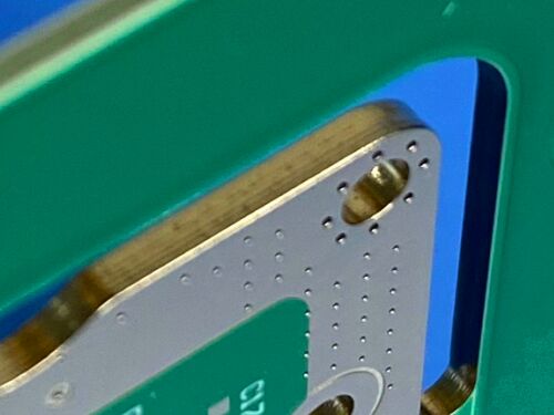
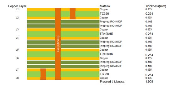
Этот ПКБ представляет собой 8-слойную медную конструкцию, использующую высокопроизводительную комбинацию материалов и строгие стандарты производства для удовлетворения требований высоконадежных электронных приложений.Он имеет смолой заполненные и закрытые проемы, облицовка краев (металлическая обшивка краев), погруженная золотая поверхность и зеленая сварная маска с белым шелковым экраном, обеспечивающая отличную целостность сигнала, тепловую производительность и механическую прочность.
Спецификации основных PCB
| Параметр конструкции |
Спецификация |
| Базовый материал |
TC350, FR408HR, RO4450F Препрег |
| Количество медных слоев |
8 слоев |
| Вес меди |
1 унция на слой |
| Толщина готовой доски |
20,0 мм |
| Размеры доски |
99 мм × 83 мм |
| Поверхностная отделка |
Золото погружения (ENIG) |
| Маска и шелкопряда |
Двусторонний: зеленая сварная маска и белый шелкоплот |
| Через конфигурацию |
Скрытые проемы; проемы 0,2 мм с наполнением смолой и электромагнитным покрытием (через заполнение и покрытие) |
| Особая особенность |
Окрашивание краев (оболочка металлических краев) |

Введение в материал TC350
TC350представляет собой керамически заполненный композит из ПТФЭ, сделанный из стекловолокна, обладающий исключительной теплопроводностью (1,0 Вт/мК), повышающей теплопередачу,уменьшает диэлектрические и вставные потериОн обрабатывает большую мощность, минимизирует горячие точки и подходит для приложений с ограниченным тепловым управлением.
Ламинаты TC350 сохраняют отличную постоянную диэлектрическую стабильность (-9 ppm/oC) при широких температурах, что критично для усилителей мощности, антенн и устройств, чувствительных к фазе/импеданции.Его низкий Z-направления CTE совпадает мед (обеспечение покрытия через отверстие надежность), и как "мягкая подложка", она устойчива к вибрациям и ударам, чтобы соответствовать стандартам испытаний на падение.
Он сильно связывается с медным низкопрофильным металлом микроволнового класса (не требуется "зубчатый мед"), что еще больше уменьшает потерю вставки при высоких частотах RF / микроволновых.его легче просверлить, чем традиционные ламинаты, и он обладает высокой прочностью кожуры для надежной адгезии меди в условиях теплового напряжения..
Ключевые характеристики и преимущества TC350
"Лучшая в своем классе" теплопроводность (1,0 W/mK) и постоянная диэлектрическая стабильность при широких температурах (-9 ppm/oC)
- Очень низкая потеря тангенса, обеспечивающая более высокую эффективность усилителя или антенны
- экономически эффективный для коммерческих применений
- Легче просверлить, чем традиционные коммерческие ламинаты с толстым, плотным тканым стеклом
- высокая прочность на очистку для надежного сцепления меди при тепловых нагрузках
- Отличные возможности рассеивания тепла и управления теплом
-Улучшенная эффективность обработки и общая надежность
- Доступен в больших размерах панелей, что позволяет использовать несколько схем для снижения затрат на обработку
TC350 Типичные применения
- Усилители мощности, фильтры и соединители
- Усилители на башне (TMA) и усилители на башне (TMB)
- Антенны с тепловым циклом, чувствительные к диэлектрическому дрейфу
- Микроволновой комбинатор и разделители мощности
Введение в материал FR408HR
FR408HR представляет собой высокопроизводительную смоловую систему FR-4 с температурой стеклянного перехода (Tg) 230°C (DMA),специально разработанные для многослойных ПКБ, требующих максимальной тепловой производительности и надежностиИзготовленная с использованием запатентованной высокопроизводительной многофункциональной смоловой системы Isola, усиленной стеклянной тканью электрического класса (E-стекло),FR408HR обеспечивает улучшение расширения оси Z на 30% и предлагает на 25% больше электрической пропускной способности (меньшие потери) по сравнению с конкурирующими продуктами в той же категории.
Материал обладает превосходной устойчивостью к влаге во время процессов повторного потока, преодолевая разрыв между требованиями к тепловой и электрической производительности.обеспечение максимальной совместимости с системами автоматизированной оптической инспекции (AOI)Он полностью соответствует требованиям RoHS и предлагает отличную совместимость с стандартными производственными процессами FR-4,облегчение интеграции в существующие производственные линии.
FR408HR Типичные применения
- многослойные ПХБ, требующие высокой тепловой производительности и надежности
- применения для сборки без свинца
-Электронные устройства с плотной компоновкой компонентов (0,8 мм возможности откида)
- ПКБ, требующие совместимости с AOI и точного изображения сварной маски
- высоконадежные электронные системы, подверженные многократным циклам обратного потока
Что такое Via Filled and Capped (покрытие, заполненное смолой и электроплатированным)?
Via filled and capped, также известный как смолой заполненный и электропластированный каппинг, является специализированным производственным процессом ПКБ, предназначенным для повышения надежности и производительности vias,особенно в условиях высокой плотностиЭтот процесс включает в себя два ключевых этапа: наполнение смолой и покрытие электропластировкой.
Во-первых, проемы (в этом PCB, 0,2 мм слепые проемы) заполняются высокотемпературной устойчивой, изолирующей смолой.который предотвращает поглощение влагиИспользуемая смола обычно совместима с ламинированием ПКБ и температурой обратного потока.поддержание стабильности во время последующих производственных процессов.
После отверждения смолы выполняется второй этап - электропластировка.наполненной смолой с помощью, образуя гладкую, плоскую крышку, которая совпадает с поверхностью ПКБ. Эта крышка защищает смолу от повреждений во время сборки, обеспечивает электрическую непрерывность (при необходимости),и обеспечивает плоскую поверхность для монтажа компонентов, что имеет решающее значение для конструкций ПКБ с высокой плотностью с тонкими компонентами.
Основные преимущества заполненной и закрытой формы включают: предотвращение проникновения сварки в проемы во время сборки, снижение отражения сигнала и перекрестного звука в высокоскоростных приложениях,повышение теплопроводности, защищая проходы от факторов окружающей среды (влажность, пыль) и улучшая общую механическую прочность ПХБ.
Роль облицовки краев
Облицовка краев, также называемая обертыванием металлических краев, является производственным процессом ПКБ, который включает облицовка обнаженных краев ПКБ проводящим металлом (обычно медью,Затем такая же поверхностная отделка, как и у ПХБ (в данном случае золото погружения)Этот процесс играет решающую роль в повышении производительности, надежности и производимости ПХБ, с следующими ключевыми функциями:
Улучшенное заземление и защита от EMI: облицовка краев образует непрерывный проводящий периметр (клетка Фарадея), повышая целостность заземления, уменьшая внешние EMI,и предотвращение внутреннего излучения сигнала, радиочастотных и микроволновых приложений, требующих превосходной целостности сигнала.
Улучшенная механическая прочность: повышает механическую прочность печатных плат, устойчивость к щелчкам, трещинам и повреждениям во время обращения, сборки и эксплуатации,специально подходящий для суровой или высокоупорной среды.
Улучшенное тепловое рассеивание: в качестве дополнительного теплового пути он рассеивает тепло компонентов, оптимизирует тепловое управление, снижает температуру соединения и продлевает срок службы компонентов.
Упрощенная электрическая непрерывность: позволяет обеспечивать электрическую непрерывность между слоями, упрощает конструкцию заземления, обеспечивает постоянную производительность и уменьшает сопротивление краев для улучшения целостности сигнала.
Улучшенная сварная способность и сборка: гладкая проводящая поверхность облегчает сварку компонентов / соединителей, установленных на краю, повышает надежность сборки и снижает риск отказа сварного соединения.

 Ваше сообщение должно содержать от 20 до 3000 символов!
 Russian